
In the realm of electronics manufacturing, ensuring the quality and reliability of electronic components and assemblies is of utmost importance. One of the most crucial techniques in this regard is X Ray Inspection. As a leading X Ray Inspection supplier, I am often asked about the resolution of X Ray Inspection in electronics. In this blog post, I will delve into the concept of resolution in X Ray Inspection, its significance in electronics, and how it impacts the overall inspection process.
Understanding Resolution in X Ray Inspection
Resolution in X Ray Inspection refers to the ability of the X Ray system to distinguish between two adjacent objects or features. It is a measure of the smallest detail that can be accurately imaged by the system. In the context of electronics, high resolution is essential for detecting and analyzing minute defects, such as cracks, voids, and misalignments in electronic components and printed circuit boards (PCBs).
There are two main types of resolution in X Ray Inspection: spatial resolution and contrast resolution.
Spatial Resolution
Spatial resolution is the ability to distinguish between two closely spaced objects in the X Ray image. It is typically measured in line pairs per millimeter (lp/mm) or micrometers (μm). A higher spatial resolution means that the X Ray system can detect smaller features and provide more detailed images. For example, a system with a spatial resolution of 10 lp/mm can distinguish between two objects that are 0.1 mm apart, while a system with a resolution of 20 lp/mm can detect objects that are only 0.05 mm apart.
Several factors affect the spatial resolution of an X Ray system, including the focal spot size of the X Ray tube, the detector pixel size, and the geometric magnification of the imaging setup. A smaller focal spot size and detector pixel size generally result in higher spatial resolution. However, reducing these parameters also has limitations, as it can lead to decreased X Ray intensity and longer exposure times.
Contrast Resolution
Contrast resolution is the ability to distinguish between objects with similar X Ray absorption properties. It is determined by the dynamic range of the detector and the ability of the X Ray system to detect small differences in X Ray attenuation. In electronics, contrast resolution is crucial for detecting defects that may not be visible based on spatial resolution alone, such as delaminations and internal voids.
A high contrast resolution allows for better visualization of these subtle defects, enabling more accurate defect analysis and classification. To improve contrast resolution, X Ray systems often use advanced imaging techniques, such as digital subtraction and phase contrast imaging. These techniques enhance the visibility of low-contrast features by highlighting the differences in X Ray absorption between the defect and the surrounding material.
Significance of Resolution in Electronics Inspection
In the electronics industry, the demand for smaller, more complex, and higher-performance components is constantly increasing. As a result, the size of electronic features, such as solder joints, vias, and integrated circuits, has decreased significantly. This trend has made it increasingly challenging to detect and inspect defects using traditional inspection methods.


X Ray Inspection with high resolution plays a vital role in meeting these challenges. It allows manufacturers to detect and analyze defects at the microscopic level, ensuring the quality and reliability of electronic products. Here are some key areas where high-resolution X Ray Inspection is essential in electronics:
Solder Joint Inspection
Solder joints are critical components in electronic assemblies, as they provide electrical and mechanical connections between components and PCBs. Defects in solder joints, such as voids, cracks, and insufficient wetting, can lead to electrical failures and reduced product reliability. High-resolution X Ray Inspection can detect these defects with high accuracy, enabling manufacturers to identify and correct issues early in the production process.
PCB Inspection
Printed circuit boards are the backbone of electronic devices, and any defects in the PCB can have a significant impact on the performance and functionality of the product. X Ray Inspection can detect a wide range of PCB defects, including shorts, opens, misaligned vias, and delaminations. By using high-resolution X Ray systems, manufacturers can ensure the integrity of the PCB and prevent costly failures in the field.
Component Inspection
Electronic components, such as integrated circuits, capacitors, and resistors, are becoming increasingly miniaturized and complex. High-resolution X Ray Inspection can be used to inspect these components for internal defects, such as die cracks, wire bond failures, and package delaminations. This helps manufacturers to identify defective components before they are assembled into the final product, reducing the risk of product recalls and warranty claims.
Comparison with Other Nondestructive Inspection Methods
While X Ray Inspection is a powerful tool for electronics inspection, it is not the only nondestructive inspection method available. Other common methods include Dye Penetrant Inspection, Ultrasonic Flaw Detection, and Magnetic Powder Inspection. Each method has its own advantages and limitations, and the choice of inspection method depends on the specific application and requirements.
Dye Penetrant Inspection
Dye Penetrant Inspection is a surface inspection method that is used to detect open defects, such as cracks and porosity, on the surface of non-porous materials. It involves applying a colored dye to the surface of the material, allowing it to penetrate into the defects, and then removing the excess dye. A developer is then applied to the surface to make the defects visible.
While Dye Penetrant Inspection is a simple and cost-effective method, it is limited to detecting surface defects and cannot provide information about internal defects. In contrast, X Ray Inspection can detect both surface and internal defects, making it a more comprehensive inspection method for electronics.
Ultrasonic Flaw Detection
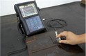
Ultrasonic Flaw Detection is a widely used nondestructive testing method that uses high-frequency sound waves to detect internal defects in materials. It is particularly effective for detecting defects in metals and composites. Ultrasonic waves are transmitted into the material, and any defects in the material will cause the waves to reflect or scatter. By analyzing the reflected or scattered waves, the location and size of the defects can be determined.
However, Ultrasonic Flaw Detection has limitations when it comes to inspecting electronic components and PCBs. The complex geometry and heterogeneous nature of these materials can make it difficult to interpret the ultrasonic signals accurately. X Ray Inspection, on the other hand, can provide clear and detailed images of the internal structure of electronic components and PCBs, making it a more suitable method for electronics inspection.
Magnetic Powder Inspection
Magnetic Powder Inspection is a nondestructive testing method that is used to detect surface and near-surface defects in ferromagnetic materials. It involves applying a magnetic field to the material and then sprinkling magnetic powder on the surface. Any defects in the material will cause the magnetic field to distort, and the magnetic powder will accumulate at the defect sites, making them visible.
Like Dye Penetrant Inspection, Magnetic Powder Inspection is limited to detecting surface and near-surface defects and cannot provide information about internal defects. X Ray Inspection, with its ability to penetrate through the material and provide detailed images of the internal structure, is a more effective method for inspecting electronic components and assemblies.
Our X Ray Inspection Solutions
As an X Ray Inspection supplier, we understand the importance of high resolution in electronics inspection. That's why we offer a range of advanced X Ray Inspection systems that are designed to meet the specific needs of the electronics industry. Our systems feature high spatial and contrast resolution, allowing for the detection of even the smallest defects in electronic components and PCBs.
We use state-of-the-art technology and innovative imaging techniques to ensure the highest level of inspection accuracy and reliability. Our X Ray systems are equipped with high-performance X Ray tubes, detectors, and image processing software, enabling us to provide clear and detailed images with excellent contrast and resolution.
In addition to our standard X Ray Inspection systems, we also offer customized solutions to meet the unique requirements of our customers. Our team of experienced engineers and technicians can work closely with you to develop a tailored inspection solution that fits your specific application and budget.
Contact Us for Procurement and Consultation
If you are looking for a reliable X Ray Inspection solution for your electronics manufacturing process, we would be happy to help. Our team of experts can provide you with detailed information about our products and services, as well as offer professional advice on the best inspection solution for your needs.
Whether you are a small-scale manufacturer or a large multinational corporation, we are committed to providing you with the highest level of quality and service. Contact us today to start a discussion about your X Ray Inspection requirements and explore how our solutions can help you improve the quality and reliability of your electronic products.
References
- ASNT (American Society for Nondestructive Testing). Nondestructive Testing Handbook, Volume 1: Radiography.
- ASTM (American Society for Testing and Materials). Standard Practice for Radiographic Examination of Weldments.